- 您现在的位置:买卖IC网 > Sheet目录473 > MAX2830EVKIT+ (Maxim Integrated)KIT EVAL FOR MAX2830
�� �
�
�MAX2830�
�2.4GHz� to� 2.5GHz� 802.11g/b� RF� Transceiver,� PA,�
�and� Rx/Tx/Antenna� Diversity� Switch�
�Pin� Description� (continued)�
�PIN�
�35�
�36�
�37�
�38�
�39�
�40�
�41�
�42�
�43�
�44�
�45�
�46�
�47�
�48�
�—�
�NAME�
�RXBBQ-�
�RXBBQ+�
�RXBBI-�
�RXBBI+�
�V� CCRXVGA�
�RXHP�
�V� CCRXFL�
�TXBBQ-�
�TXBBQ+�
�TXBBI-�
�TXBBI+�
�V� CCRXMX�
�ANTSEL�
�RXTX�
�EP�
�FUNCTION�
�Receiver� Baseband� Q-Channel� Differential� Outputs.� In� TX� calibration� mode,� these� pins� are� the� LO� leakage�
�and� sideband� detector� outputs.�
�Receiver� Baseband� I-Channel� Differential� Outputs.� In� TX� calibration� mode,� these� pins� are� the� LO� leakage�
�and� sideband� detector� outputs.�
�Receiver� VGA� Supply� Voltage�
�Receiver� Baseband� AC-Coupling� High-Pass� Corner� Frequency� Control� Logic� Input�
�Receiver� Baseband� Filter� Supply� Voltage�
�Transmitter� Baseband� I-Channel� Differential� Inputs�
�Transmitter� Baseband� Q-Channel� Differential� Inputs�
�Receiver� Downconverters� Supply� Voltage�
�Antenna� Selection� Logic� Input.� See� Table� 1� for� operation�
�Rx/Tx� Mode� Control� Logic� Input.� See� Table� 32� for� operating� modes.�
�Exposed� Paddle.� Connect� to� the� ground� plane� with� multiple� vias� for� proper� operation� and� heat� dissipation.�
�Do� not� share� with� any� other� pin� grounds� and� bypass� capacitors'� ground.�
�Detailed� Description�
�The� MAX2830� single-chip,� low-power,� direct� conversion,�
�zero-IF� transceiver� is� designed� to� support� 802.11g/b�
�MAX2830�
�applications� operating� in� the� 2.4GHz� to� 2.5GHz� band.�
�The� fully� integrated� transceivers� include� a� receive� path,�
�transmit� path,� VCO,� sigma-delta� fractional-N� synthesizer,�
�crystal� oscillator,� RSSI,� PA� power� detector,� temperature�
�sensor,� Rx� and� Tx� I/Q� error-detection� circuitry,� baseband-�
�control� interface,� linear� power� amplifier,� and� an� Rx/Tx�
�antenna� diversity� switch.� The� only� additional� components�
�required� to� implement� a� complete� radio� front-end� solution�
�are� a� crystal,� a� pair� of� baluns,� a� BPF,� and� a� small� number�
�of� passive� components� (RCs,� no� inductors� required).�
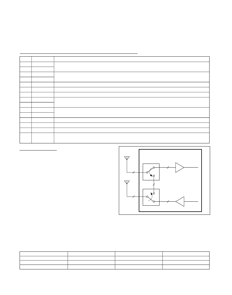
�Rx/Tx� and� Antenna� Diversity� Switches�
�The� MAX2830� integrates� an� Rx/Tx� switch� and� an� anten-�
�na� diversity� switch� before� the� receiver� and� after� the�
�2�
�ANT1�
�2�
�ANT2�
�2�
�2�
�2�
�LNA�
�PA�
�power� amplifier.� See� Figure� 1� for� a� block� diagram� of� the�
�switches.� The� receiver� and� transmitter� enable� pin�
�(RXTX)� and� the� antenna� selection� pin� (ANTSEL)� deter-�
�mine� which� ports� (ANT1� or� ANT2)� the� receiver� or� trans-�
�mitter� is� connected� to.� See� Table� 1� for� the� Rx/Tx� and�
�antenna� diversity� switches� truth� table.� When� RXTX� =� 0�
�Figure� 1.� Simplified� Rx/Tx� and� Antenna� Diversity� Switch� Structure�
�(receive� mode)� and� ANTSEL� =� 0,� the� switch� provides� a�
�low-insertion� loss� path� (main)� between� the� ANT1� port�
�(pins� 4� and� 5)� and� the� receiver.� When� RXTX� =� 0�
�(receive� mode)� and� ANTSEL� =� 1,� the� switch� provides�
�Table� 1.� Rx/Tx� and� Antenna� Diversity� Switches� Operation�
�20�
�RXTX�
�0�
�0�
�1�
�ANTSEL�
�0�
�1�
�X�
�MODE�
�Rx� (main)�
�Rx� (diversity)�
�Tx�
�ANTENNA�
�Ant1_�
�Ant2_�
�Ant2_�
�Maxim� Integrated�
�发布紧急采购,3分钟左右您将得到回复。
相关PDF资料
MAX2831EVKIT+
KIT EVAL FOR MAX2831
MAX2837EVKIT+
KIT EVAL FOR MAX2837
MAX2838EVKIT+
KIT EVAL FOR MAX2838
MAX2839ASEVKIT+
KIT EVAL FOR MAX2839A WLP
MAX2839EVKIT+
KIT EVAL FOR MAX2839
MAX2851ITK+
TRANSMITTER MIMO 5GHZ 5CH 68TQFN
MAX2852ITK+
IC RECEIVER DFS 5GHZ 68TQFN
MAX2870EVKIT#
EVAL KIT MAX2870
相关代理商/技术参数
MAX2830SEWU
功能描述:射频收发器
RoHS:否 制造商:Atmel 频率范围:2322 MHz to 2527 MHz 最大数据速率:2000 Kbps 调制格式:OQPSK 输出功率:4 dBm 类型: 工作电源电压:1.8 V to 3.6 V 最大工作温度:+ 85 C 接口类型:SPI 封装 / 箱体:QFN-32 封装:Tray
MAX2830SEWU+
功能描述:射频收发器
RoHS:否 制造商:Atmel 频率范围:2322 MHz to 2527 MHz 最大数据速率:2000 Kbps 调制格式:OQPSK 输出功率:4 dBm 类型: 工作电源电压:1.8 V to 3.6 V 最大工作温度:+ 85 C 接口类型:SPI 封装 / 箱体:QFN-32 封装:Tray
MAX2831ETM+
功能描述:射频收发器 2.4-2.5GHz 802.11g/b 射频收发器 RoHS:否 制造商:Atmel 频率范围:2322 MHz to 2527 MHz 最大数据速率:2000 Kbps 调制格式:OQPSK 输出功率:4 dBm 类型: 工作电源电压:1.8 V to 3.6 V 最大工作温度:+ 85 C 接口类型:SPI 封装 / 箱体:QFN-32 封装:Tray
MAX2831ETM+T
功能描述:射频收发器 2.4-2.5GHz 802.11g/b 射频收发器 RoHS:否 制造商:Atmel 频率范围:2322 MHz to 2527 MHz 最大数据速率:2000 Kbps 调制格式:OQPSK 输出功率:4 dBm 类型: 工作电源电压:1.8 V to 3.6 V 最大工作温度:+ 85 C 接口类型:SPI 封装 / 箱体:QFN-32 封装:Tray
MAX2831EVKIT+
功能描述:WiFi/802.11开发工具 MAX2831 Eval Kit RoHS:否 制造商:Roving Networks 产品:Evaluation Boards 工具用于评估:RN-171 支持协议:802.11 b/g 频率:2.4 GHz 接口类型:UART 工作电源电压:2 V to 16 V
MAX2832ETM+
制造商:Maxim Integrated Products 功能描述:2.4GHZ TO 2.5GHZ, 802.11G RF TRANSCEIVER 制造商:Maxim Integrated Products 功能描述:IC+MAX2832ETM+ - Rail/Tube
MAX2832ETM+CFK
制造商:Maxim Integrated Products 功能描述:2.4GHZ TO 2.5GHZ, 802.11G RF TRANSCEIVERS WITH INTEGRATED PA - Rail/Tube
MAX2832ETM+T
制造商:Maxim Integrated Products 功能描述:2.4GHZ TO 2.5GHZ, 802.11G RF TRANSCEIVER 制造商:Maxim Integrated Products 功能描述:2.4GHZ TO 2.5GHZ, 802.11G RF TRANSCEIVERS WITH INTEGRATED PA - Tape and Reel